If you've ever used a smartphone, driven a car with advanced sensors, or relied on a medical device, chances are you've benefited from the silent hero behind the scenes—the Printed Circuit Board (PCB). These boards are the unsung backbone of nearly every electronic device we use today. Though often invisible to the end user, PCBs are absolutely essential for making modern electronics work efficiently and reliably.
In simple terms, PCB design is where electronics come to life. It's the art and science of organizing all the tiny components that power your devices onto a board that not only fits—but functions flawlessly. And as technology continues to evolve rapidly, so does the complexity and importance of PCB design.
From enabling lightning-fast 5G connectivity to powering smart homes and AI-driven machines, modern PCBs are expected to be smaller, faster, and more powerful than ever before. Getting the design right isn’t just important—it’s critical.
In this guide, we’ll walk you through the basics of PCB design, explore its key components, and unpack why it matters more than ever in today’s connected world.
What is PCB Design?
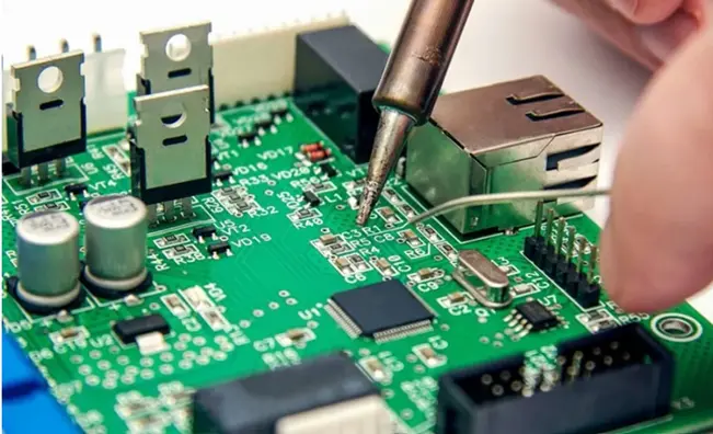
At its core, PCB design is the process of planning and building the “map” that allows an electronic device to function. A Printed Circuit Board (PCB) isn’t just a platform—it’s the lifeline that connects and powers every component inside a device, from microchips and resistors to capacitors and connectors.
Think of it as the architectural blueprint of an electronic system. Just as an architect designs a house with rooms, walls, and electrical wiring, a PCB designer lays out components and draws copper paths (called traces) that guide electrical signals across the board.
This entire process takes place on a thin, non-conductive base—usually made of fiberglass or composite epoxy—onto which conductive copper layers are laminated. Designing a PCB requires a mix of engineering know-how, design software skills, and a clear understanding of manufacturing limitations and standards.
Here are the key stages involved in PCB design:
1. Schematic Capture
This is where it all begins. Engineers create a digital circuit diagram, showing how every electronic component is connected. It's like the electrical blueprint of the system, a high-level map that lays the foundation for the physical layout.
2. Component Placement
Once the schematic is ready, it’s time to move the components into position. Designers must place each chip, resistor, and connector carefully to optimize space, ensure proper signal flow, and manage heat dissipation. The goal is a compact yet efficient layout.
3. Routing
Routing is the process of drawing copper traces that connect the pins of components, allowing electrical signals to flow smoothly. It’s a meticulous task that requires precision and planning, especially to avoid crosstalk, interference, or signal delays, issues that can compromise performance.
4. Design Rule Check (DRC)
Before finalizing the design, software tools run a set of automated checks to catch potential errors like traces that are too close, missing connections, or violations of spacing rules. These DRC checks help ensure the board will function properly and be producible.
5. Gerber File Generation
Once everything checks out, the design is exported as a set of Gerber files standardized formats used by PCB manufacturers. These files contain precise information about each layer of the board, including copper patterns, drill holes, solder masks, and silkscreen labels.
Whether you're working on a simple hobby project or a multi-layer industrial-grade board, good PCB design is what turns an idea into a working product. It bridges the gap between electrical theory and real-world technology.
Why is PCB Design So Important?
In a world where electronics power nearly every aspect of our lives, PCB design is more than just a technical step—it’s the foundation of innovation. A well-designed printed circuit board can make the difference between a product that excels and one that fails prematurely. Here’s why PCB design plays such a vital role in today’s technology-driven world:
1. It’s the Foundation of All Modern Electronics
From wearable fitness trackers to industrial control systems, PCBs are at the heart of virtually every electronic device. They physically support and electrically connect all components such as processors, sensors, memory chips, and more. If the PCB is poorly designed, even the most advanced components can’t perform at their best. A good layout ensures everything runs smoothly, reliably, and as intended.
2. Enables Miniaturization and High Performance
Today’s gadgets are becoming smaller, sleeker, and more powerful. PCB design makes this possible by allowing engineers to pack dense circuits into compact spaces without compromising performance or signal quality. Think of how a smartphone packs in cameras, processors, wireless modules, and a battery, all within millimeters. That's smart PCB engineering at work.
3. Improves Manufacturability and Reduces Costs
A thoughtful PCB layout doesn’t just work better, it’s easier and cheaper to manufacture. When component placement, routing, and spacing are optimized, automated assembly lines can fabricate and assemble boards more efficiently, with fewer errors and less waste. For companies producing thousands of units, this means big savings and faster turnaround.
4. Preserves Signal Integrity and Controls EMI
As electronics push into high-speed data and RF applications, signal integrity becomes mission-critical. Poor routing can lead to noise, interference, or data corruption. Good PCB design incorporates controlled impedance, proper grounding, shielding, and trace spacing to minimize electromagnetic interference (EMI) and ensure stable, accurate signals, even at gigahertz frequencies
5. Manages Heat for Long-Term Reliability
Electronic components generate heat and if that heat isn't managed properly, it can degrade performance or cause permanent failure. PCB designers use thermal vias, copper pours, and heat sinks to dissipate heat efficiently, especially in power electronics, LEDs, and motor controllers. A thermally-aware design keeps your product running cool and safe.
6. Ensures Safety and Regulatory Compliance
Safety is non-negotiable. A professionally designed PCB follows industry standards like IPC, UL, and RoHS to ensure it’s safe for use and environmentally compliant. That means proper clearances, creepage distances, insulation, and fire-retardant materials, all critical in industries like medical, automotive, and aerospace.
7. Supports Scalability and Future Upgrades
A well-planned PCB layout not only works today, it’s built for tomorrow. With smart design choices like modular sections, test points, and expansion headers, your board becomes easier to debug, maintain, and upgrade. That flexibility is gold for startups, OEMs, and R&D teams who need to iterate fast or scale up production.
Applications Across Industries
PCB design plays a critical role across a wide range of industries, each with its own unique requirements and challenges.
Consumer Electronics
- Used in smartphones, TVs, and wearables, PCBs enable compact, power-efficient, and aesthetically optimized devices.
- Designs focus on miniaturization, cost-efficiency, and high-volume manufacturability.
Automotive
- PCBs control systems like ADAS, infotainment, and battery management in modern vehicles.
- They must withstand high temperatures, vibration, and meet strict reliability standards.
Medical Devices
- Found in pacemakers, monitors, and diagnostic tools, medical PCBs require extreme reliability and precision.
- They must be compact, biocompatible, and meet rigorous regulatory compliance.
Industrial Automation
- Used in PLCs, robotics, and motor drivers, these PCBs operate in harsh environments.
- Designs emphasize durability, real-time performance, and long lifecycle support.
Aerospace and Defense
- PCBs in avionics and defense systems must be ultra-reliable and mission-critical.
- They are built to handle thermal extremes, radiation, and meet military-grade standards.
Renewable Energy
- Essential in solar inverters and wind systems, these PCBs manage high power and voltage.
- They require efficient heat dissipation and long-term field reliability.
The Role of Innovation in PCB Design
At Electronics Interconnect Engineering, we understand that PCB design is not just a technical task, it's an innovation driver. By leveraging advanced CAD tools, simulation software, and real-world testing, we ensure our designs meet both functional and market demands. Our team stays at the forefront of industry standards, continually pushing the boundaries to create smarter, more efficient, and more reliable electronic systems.
Explore more insights on cutting-edge electronics at our Innovation Hub, where we share knowledge, trends, and expertise on interconnect technologies and design best practices.
Conclusion
PCB design forms the foundation of modern electronics. From basic gadgets to life-saving equipment, a robust PCB layout ensures performance, safety, and efficiency. As technology continues to evolve, the demand for intelligent, compact, and reliable PCB solutions will only grow. Investing in good PCB design today means shaping the future of electronics tomorrow.