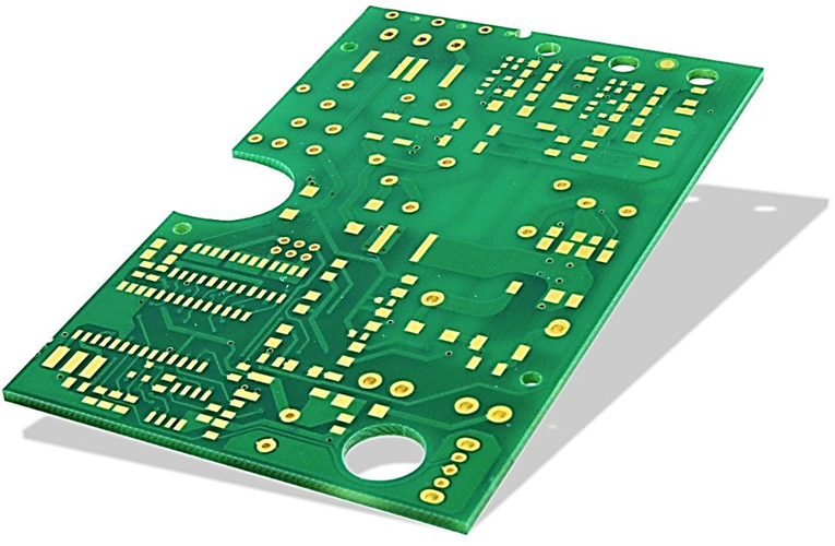
1. Fundamentals of PCB Design
PCB design transforms electrical schematics into manufacturable circuit boards. Modern design requires understanding both electrical theory and manufacturing constraints.
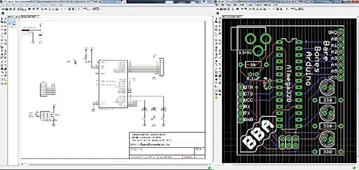
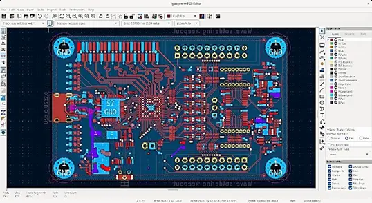
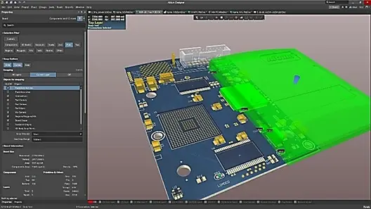
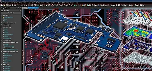
1.1. Modern CAD Tools
Most Popular Tools used today:
NAME |
MANUFACTURER |
STRONGEST FEATURE |
|
ALLEGRO |
CADENCE |
ADVANCED ROUTING FOR HIGH-SPEED |
|
ALTIUM |
ALTIUM |
ALL-IN-ONE ENVIRONMENT |
|
PADS |
SIEMENS |
STRONG SIGNAL INTEGRITY ANALYSIS |
|
EAGLE |
AUTODESK |
INTEGRATION WITH FUSION 360 |
|
KICAD |
OPEN SOURCE |
FREE, OPEN-SOURCE |
1.2 Industry Standards:
STANDARD |
TITLE |
|
IPC-2221 |
GENERIC STANDARD ON PRINTED BOARD DESIGN |
|
IPC-2222 |
DESIGN STANDARD FOR RIGID ORGANIC PRINTED BOARDS |
|
IPC-6012 |
QUALAND PERF SPEC FOR RIGID PRINTED BOARDS |
|
IPC-A-610 |
ACCEPTABILITY OF ELECTRONIC ASSEMBLIES |
|
IPC-2226 |
DESIGN STANDARD FOR HIGH DENSITY INTERCONNECT (HDI) |
|
IPC-4101 |
SPEC FOR BASE MATERIALS FOR RIGID PRINTED BOARDS |
|
IPC-6013 |
QUAL AND PERF SPEC FOR FLEXIBLE PRINTED BOARDS |
|
IPC-2152 |
CURRENT CARRYING CAPACITY IN PRINTED BOARD DESIGN |
|
UL 796 |
SAFETY FOR PRINTED-WIRING BOARDS |
|
IPC-7351 |
GENERIC REQUIREMENTS FOR SURFACE MOUNT DESIGN |
1.3. Core Material and Substrate
FR-4
A fiberglass-reinforced epoxy laminate, widely used for its balance of cost, mechanical strength, and thermal resistance (up to ~140°C). It is chemically resistant, easy tomanufacture, and suitable for most applications.
POLYIMIDE
Offers superior flexibility and high-temperature endurance (up to 260°C or more), making it ideal for flexible circuits and harsh environments. Polyimide has a lower dielectric constant and excellent chemical resistance but is more expensive.
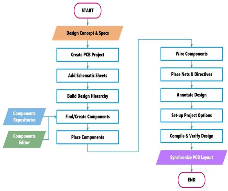
1.4. Design Workflow
PCB Design Process
- Schematic Creation Draw the circuit diagram in PCB design software.
- Placement Place electronic components on the board layout.
- Routing Connect components with copper traces
- DRC Run automated checks
- Gerbers Export files Generation (Gerber, drill, etc.)
- Production Manufacturing PCB
- Assembly Pick and Place (PCBA)
2. Design Preparation
Effective PCB design begins with thorough preparation and analysis.
2.1. Schematic Analysis
Critical Schematic Review Elements
- Net connectivity - Verify all connections are intentional
- Power requirements - Identify supply voltages and currents
- Signal types - Classify analog, digital, and power nets
- Critical paths - Locate timing-sensitive connections
2.2. Component Selection
Package considerations for layout:
PACKAGE |
PITCH |
LAYOUT DIFFICULTY |
THERMAL PERFORMANCE |
|
SOIC |
1.27MM |
LOW |
GOOD |
|
QFP |
0.8MM |
MEDIUM |
FAIR |
|
BGA |
0.5-1.0MM |
HIGH |
EXCELLENT |
|
QFN |
0.5MM |
MEDIUM |
EXCELLENT |
2.3. Board Planning
Essential Planning Steps
- Board outline - Define mechanical constraints (DXF)
- Layer count - Determine based on routing density
- Component groups - Organize by function (power, analog, digital)
- Connector placement - Position for system integration
3. Physical Design Parameters
Physical design parameters directly impact electrical performance.
3.1. Measurments
PCB design uses both imperial and metric units:
PARAMETER |
IMPERIAL |
METRIC |
APPLICATION |
|
DRILL SIZES |
MILS/INCHES |
MILLIMETERS |
VIA AND HOLE SIZING |
|
TRACE WIDTH |
MILS |
MICRONS |
FINE PITCH ROUTING |
|
COMPONENT PITCH |
MILS |
MILLIMETERS |
PACKAGE DIMENSIONS |
UNIT |
DEFINITION |
RATIO TO OTHER UNITS |
|
MIL |
1/1000 INCH (0.001 INCH) |
1 MIL = 0.0254 MM = 25.4 µM |
|
MM |
1/1000 METER |
1 MM = 39.37 MILS |
|
INCH |
STANDARD IMPERIAL UNIT |
1 INCH = 25.4 MM = 1000 MILS |
|
µM |
1/1,000,000 METER (0.001 MM) |
1 µM = 0.03937 MIL = 0.001 MM |
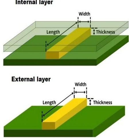
3.2 Trace Geometry
Standard trace specifications:
Minimum Teace Widths by Layer:
- Outer layers - 0.1mm (4 mil) typical
- Inner layers - 0.075mm (3 mil) typical
- High current - Calculate based on IPC-2221
Trace Spacing Requirements:
- Same net - No minimum spacing
- Different nets - 0.1mm (4 mil) minimum
- High voltage - Per IPC-2221 voltage tables
3.3. Trace Current Calculations
Calculate trace width for current carrying capacity:
IPC-2221 Formula:
- 𝐴𝑟𝑒𝑎 = (𝐶𝑢𝑟𝑟𝑒𝑛𝑡 / (𝑘 × (𝑇𝑒𝑚𝑝 𝑅𝑖𝑠𝑒)^𝑏))^(1/𝑐)
- Where k, b, c are constants based on layer type
Common Applications:
- Signal traces - 0.1-0.2mm width adequate
- Power traces - 0.5-2.0mm typical
- High current - Use copper pours or multiple vias
Example:
12V, 2A power supply requires 0.8mm trace width for 10°C temperature rise on outer layer.
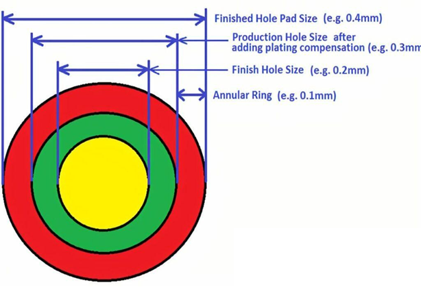
3.4. VIA Sizing
Minimum Size:
Determined by PCB manufacturer capabilities, typically 0.2–0.3 mm drill diameter.
Aspect Ratio:
Ensure via depth-to-diameter ratio supports reliable plating (commonly ≤ 8:1).
Current Capacity:
Select via size based on required current (multiple vias for high-current paths).
Signal Integrity:
Avoid placing vias in high-speed signal paths unless necessary, minimize stubs.
Clearance:
Maintain adequate spacing between vias and other features to prevent
4. Component Integration:
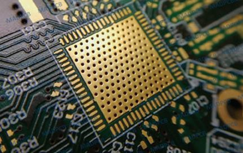
Proper component integration ensures reliable manufacturing and assembly.
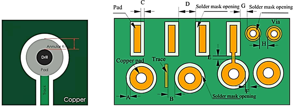
4.1. PAD Design
Pad geometry affects soldering reliability:
Standard PAD Extensions:
- SOIC packages - 0.05mm extension beyond lead
- QFP packages - 0.1mm extension for fine pitch
- BGA packages - Pad diameter 80% of ball diameter
PAD Shapes
- Round - Standard for through-hole
- Oval - Wave soldering applications
- Rectangle - Surface mount devices
- Thermal - Heat dissipation requirements
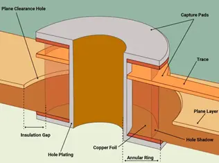
4.2. VIA Implementation
- Standard Via: Drilled through all layers
- Micro Via: Very small, laser-drilled
- Blind Via: Connects outer layer to one or more inner layers.
- Buried Via: Located entirely within inner layers\
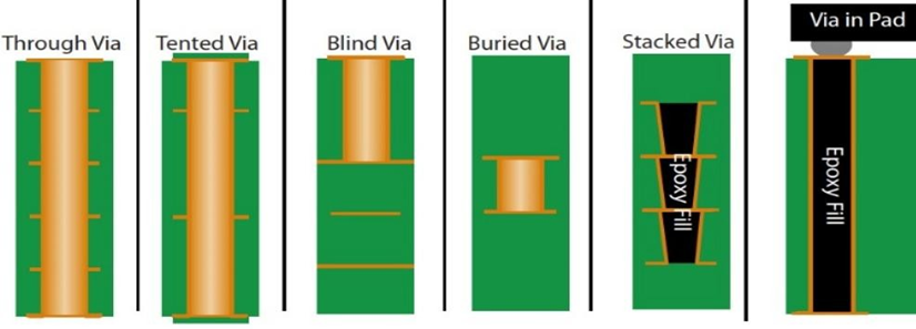
VIA Placement Guidelines:
- Signal vias - Minimize length for high-speed signals
- Power vias - Multiple vias for current distribution
- Thermal vias - Under heat-generating components
4.1. PAD Design
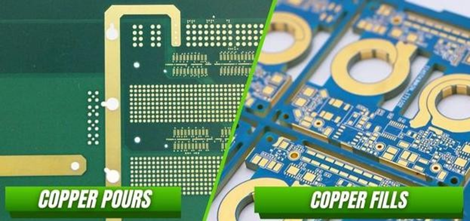
Copper Fills Provide:
- Ground planes - Low impedance return paths
- Power distribution - Reduced resistance
- EMI shielding - Noise reduction
- Thermal management - Heat spreading
Fill Strategies
- Solid fills - Maximum copper coverage
- Hatched fills - Reduced copper stress
- Thermal relief - Soldering accessibility
4.4. Other Board Features
COPPER TRACES |
CONDUCTIVE PATHS |
|
SUBSTRATE |
THE CORE MATERIAL (LIKE FR-4) |
|
SOLDER MASK |
PROTECTIVE COATING TO PREVENT SHORTS |
|
SILKSCREEN |
PRINTED MARKINGS FOR LABELS, REFDES. |
|
COMPONENTS |
PHYSICAL ELECTRONIC PARTS |
|
TEST POINTS |
DESIGNATED TESTING SPOTS |
|
MOUNTING HOLES |
MECHANICALLY SECURING THE PCB |
5. Design Rules and Constraints
Design rules ensure manufacturability and electrical performance.
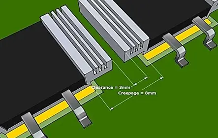
5.1. Clearance Requirements
Critical clearances for reliable operation:
Electircal Clearances:
- Trace to trace - 0.1mm minimum
- Via to trace - 0.05mm minimum
- Pad to pad - 0.1mm minimum
- High voltage - Per safety standards
Mechanical Clearances:
- Board edge - 0.5mm keep-out zone
- Mounting holes - 1.0mm clearance
- Connectors - Mating clearance required
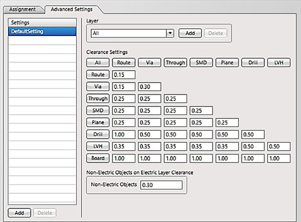
5.2. DRC Implementation
Design Rule Check categories:
Electrical Rules:
- Connectivity verification
- Net class constraints
- Power integrity checks
Physical Rules:
- Minimum trace width
- Via size verification
- Clearance validation
Manufacturing Rules:
- Drill size limitations
- Aspect ratio constraints
- Solder mask requirements
5.3. Routing Constraints
Define rules for how traces are routed on the PCB, including minimum and maximum trace widths, controlled impedance requirements, differential pair routing, and maximum trace lengths. These constraints ensure signal integrity, manufacturability, and compliance with electrical performance requirements.
5.4. Manufacturing Constraints:
Set limitations based on your PCB fabricator’s capabilities, such as minimum drill sizes, annular ring sizes, copper-to-edge clearances, and stack-up requirements. These rules ensure the design can be reliably and cost-effectively manufactured, avoiding costly redesigns and production delays.
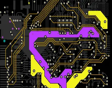
6. Layout Strategies
Strategic layout approach determines design success and efficiency.
6.1. Component Placement
Systematic placement methodology:
Phase 1 - Critical Components:
- Connectors at board edges
- Crystal oscillators near processors
- Power regulators for thermal management
- High-current components with thermal relief
Phase 2 - Funtional Groups:
- Analog circuits isolated from digital switching
- Power supply components grouped
- Decoupling capacitors near power pins
- Test points accessible
Phase 3 - Optimization:
- Minimize trace lengths for high-speed signals
- Balance component density
- Consider mechanical constraints
- Plan for thermal management

6.2 Manual Routing
Strategic routing approach:
Priority Order:
- Power and ground - Establish solid references
- Clock signals - Minimize skew and noise
- Critical analog - Avoid digital noise coupling
- High-speed digital - Control impedance and timing
- General I/O - Fill remaining connections
Routing Techniques:
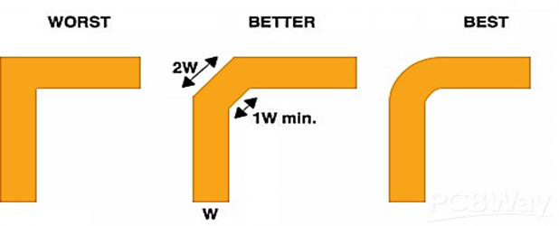
- 45-degree angles - Minimize signal reflection
- Constant width - Maintain impedance control
- Via minimization - Reduce signal disruption
- Layer transitions - Plan for signal integrity
Routing by case:
Theory | Routing Technique | Reason |
| Minimize Sharp Corners | |
High Speed | Use Gradual Curves | Reduces Reflections and EMI |
| Control Length | |
| Use Wide Traces | ||
Power | Multiple VIAS | Ensures Low Resistance |
| Solid Copper Planes | |
| Route Parallel | ||
Differential | Equal Length | Maintains Signal Integrity |
| Coupled Trace Pairs | |
| Isolate From Digital | ||
Analog | Use Guard Traces | Minimizes Noise |
| Avoid Loops | |
| Short Direct Paths | ||
RF | Controlled Impedance | Prevents Reflection and Loss |
| Avoid Stubs (Antenna) |
6.3. Layer Management
Effective layer utilization:
Two Layer Board:
- Component side for horizontal routing
- Solder side for vertical routing
- Ground plane sections where possible
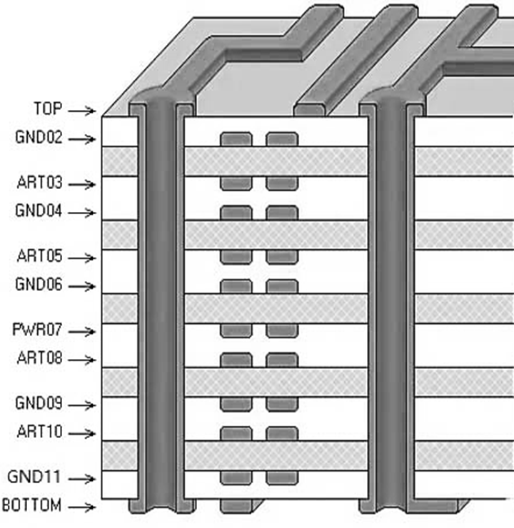
Four Layer Board:
- Layer 1: Component placement and routing
- Layer 2: Ground plane
- Layer 3: Power plane
- Layer 4: Routing and components
Six Layer Board:
- Dedicated signal layers
- Multiple power planes
- Controlled impedance requirements
- High-speed signal isolation
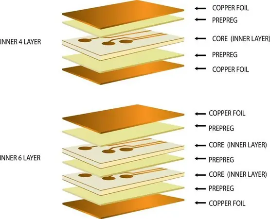
6.4. Layer Considerations:
Standard Thickness:
Most common thickness 1.57mm for 2-layer and some mid-layer counts.
Multilayer builds often range from 2.36–4.75 mm but can be customized
Layer Count Constraints:
More layers increase overall thickness and complexity.
Internal dielectric thickness (core/prepreg) must meet minimums for reliability and manufacturability. IPC-6012 requires ~2.5mil for class 3 (recommended 3-4mil)
ODD vs EVEN Layers:
Odd-numbered layer counts (e.g., 6, 11) are possible but less common due to manufacturing and lamination constraints.
Even-numbered layers are standard for symmetry, cost, and reliability.
Component Side and Bottom:
Components can be placed on both sides (top and bottom).
Some high-density designs use micro-vias and buried/blind vias for inter-layer routing.
Potential Problems in Multilayer (10+)
- Increased risk of registration errors between layers.
- Thermal management and warping become more critical.
- Signal integrity challenges (crosstalk, impedance control).
- Higher manufacturing cost and longer lead times.
- Complex stack-up management and increased risk of delamination.
7. Manufacturing
7.1. Fabrication Layers
Essential manufacturing layers:
Copper Layer:
- Signal s power distribution
- Controlled impedance
- Current carrying capacity
Solder Mask:
- Many colors available
- 0.1mm minimum feature size
- Reg. tolerance ±0.075mm
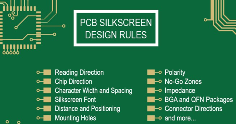
Silkscreen:
- RefDes and values
- Polarity markings and pin 1
- Assembly instructions
- Company logos (revision)
Drill Files:
- Through-hole specifications
- Via definitions
- Slot and cutout requirements
7.2. Assembly Requirements
Design for assembly guidelines:
Component Orientation:
- Consistent polarized component alignment
- IC pin 1 indicators clearly marked
- Similar components in same orientation
Silkscreen:
- Each component with its own RefDes (when possible)
- Minimum 50mil to be seen
- Avoid silk beneath components placement
Fiducial Markings:
- Minimum 3 fiducials for automated assembly
- 1mm diameter copper circles
- Clear of solder mask
- Positioned for maximum accuracy
Test Point Acccess:
- 1.27mm minimum spacing
- 0.5mm minimum diameter
- Accessible from single side preferred
Component Occupancy
- Try to avoid over 70% occupancy
- High density design (mobile) increase the risks such as thermal and integrity
- Assembly access becomes challenging in HDI design
7.3. Testing Provisions
Built-in test capabilities:
In-Circuit Testing:
- Test point accessibility
- Fixture probe clearances
- Component value verification
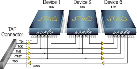
Boundary Scan:
- JTAG connectivity for digital circuits
- Test access port implementation
- Scan chain continuity
Functional Testing:
- Power supply verification
- Signal integrity checks
- Performance validation
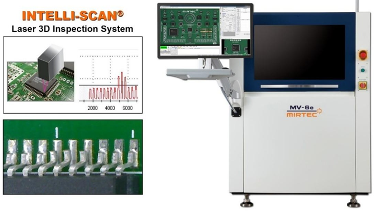
Automated Optical Inspection (AOI):
- Component placement accuracy
- Solder joint quality inspection
- Polarity and orientation verification
Burn-In Testing:
- Extended operation under stress conditions
- Early failure detection
- Reliability assessment under load
8. High Speed and Power
8.1. High Speed Constraints
Critical parameters for high-frequency design:
Transmission Line Effect:
- Controlled impedance (50Ω single-ended, 100Ω differential)
- Trace length matching for clock distributions
- Via stub elimination for frequencies >1GHz
- Ground plane continuity for return paths
Signal Integrity Techniques:
- Differential pair routing for high-speed data
- Guard traces for sensitive analog signals
- Termination networks for signal quality
- Power supply decoupling strategies
Example:
DDR4 memory interface requires matched trace lengths within 0.1mm and controlled 100Ω differential impedance for data signals.

8.2. Power Distribution
Robust power delivery systems:
Power Plane Design:
- Minimum 0.5oz copper weight for power planes
- Multiple via connections for current distribution
- Decoupling capacitor placement optimization
- Thermal management integration
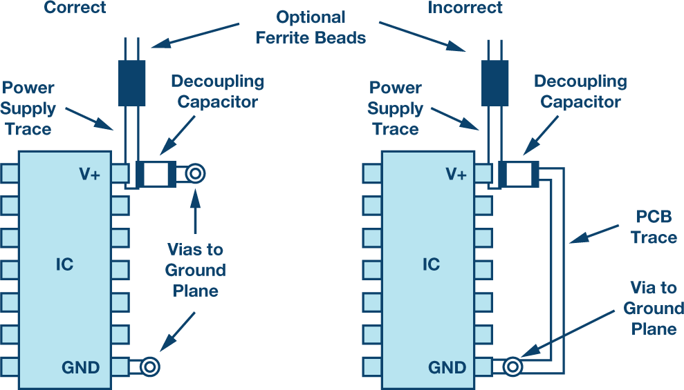
Bypass Capacitor Strategy:
- High-frequency ceramics (0.1µF) at each IC
- Medium-frequency tantalums (10µF) per circuit section
- Low-frequency electrolytics (100µF+) at power input
- ESR and ESL considerations for effectiveness
Current Density Management:
- Maximum 35A/mm² for external copper layers
- Maximum 17.5A/mm² for internal copper layers
- Thermal rise calculations per IPC-2221
- Hot spot identification and mitigation
Voltage Regulation and Distribution:
- Voltage regulator selection for stability and efficiency
- Distributed regulation for localized supply needs
- Feedback loop compensation for transient response
- Load regulation and line regulation specifications
Grounding and Return Path Optimization
- Solid ground planes for low impedance returns
- Minimized ground loops for noise reduction
- Ground stitching vias for multi-layer continuity
- Segregation of analog and digital ground domains
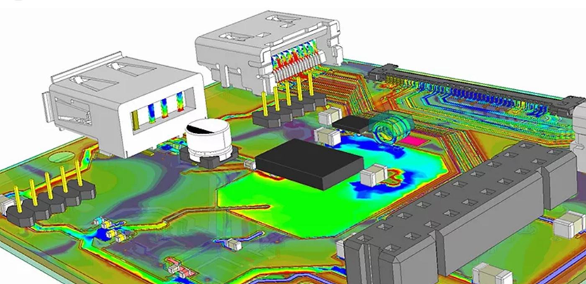
9. Signal Integrity
Signal integrity ensures reliable data transmission in high-speed digital circuits.
9.1. Transmission Line Theory
Basic Transmission Line Parameters:
- Characteristic impedance - Z₀ = √(L/C)
- Propagation delay - Critical for timing analysis
- Rise time effects - Signals behave as transmission lines when trace length > λ/10
Common Impedence Targets
- Single-ended 50Ω ±10% General digital
- Differential 100Ω ±10% High-speed data
- Coaxial 75Ω ±5% Video signals
- LVDS 100Ω ±5% Display interfaces
9.2. Crosstalk Analysis
Crosstalk Mechanisms:
- Capacitive coupling - Dominant in high-impedance circuits
- Inductive coupling - Significant in high-current switching
- Common impedance - Shared return paths
Mitigation Techniques:
- Increased spacing (3W rule minimum)
- Orthogonal routing between layers
- Differential signaling for critical nets
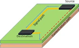
9.3. Return Path Management
Ground Plane Continuity:
- Unbroken reference planes for high-speed signals
- Via stitching across plane splits
- Minimum 0.1mm via spacing for effective stitching
Layer Transition:
- Reference plane changes require return vias
- Via placement within 200 mils of signal via
- Shortest possible via stubs
Power Supply Decoupling:
- § Multiple capacitor values for broadband filtering
- § Placement within 5mm of power pins
- § Low ESL capacitors for high-frequency performance
10. Thermal Management
Effective thermal design prevents component failure and ensures reliable operation.
10.1. Heat Transfer Principles
Thermal Resistance Calculation:
- Rth = ΔT / P (°C/W)
- Junction-to-ambient path analysis
- Multiple heat transfer paths in parallel
Efficiency Design Considerations:
- Conduction High PCB copper Thermal vias, pours
- Convection Medium Air-Cooling Component spacing
- Radiation Low High temperature Surface emissivity
10.2. Thermal VIA Design
VIA Array Calculation:
- Thermal resistance per via - Rth = 70°C/W typical
- Via spacing - 1.2mm maximum for effective heat spreading
- Fill options - Solid copper, thermal epoxy, or air-filled
Thermal VIA Specifications:
- Thermal resistance per via - Rth = 70°C/W typical
- Via spacing - 1.2mm maximum for effective heat spreading
- Fill options - Solid copper, thermal epoxy, or air-filled
Example Calculation:
- Power dissipation 5W (20°C rise) - Needs minimum 14 thermal vias of 0.2mm under IC.
10.3. Copper Pour Strategies
Heat Spreading Techniques:
- Solid copper pours under high-power components
- Thermal spoke connections to maintain solderability
- Multi-layer thermal vias for vertical heat transfer
Copper Thermal Performance
- Low-power digital 0.5oz (17μm) Basic heat spreading
- Power management 1.0oz (35μm) Standard thermal design
- High-power analog 2.0oz (70μm) Enhanced heat dissipation
- Power electronics 3.0oz+ (105μm+) Maximum thermal capacity
11. High-Speed Protocols
Contemporary digital interfaces require specific design considerations.

11.1. USB Design Guidelines
USB 2.0 Requirements:
- Differential impedance - 60Ω ±15%
- Trace length matching - ±0.1mm
- Maximum trace length - 1500mm
- Common mode choke placement
USB 3.0/3.1 Considerations:
- SuperSpeed differential pairs - 60Ω ±7Ω
- Tighter length matching - ±50μm
- Via minimization in signal path
- Enhanced shielding requirements
Design Specific Consideration:
- USB 2.0 : 480 Mbps ±0.1mm EMI filtering
- USB 3.0 : 5 Gbps ±50μm Separate SS pairs
- USB 3.1 : 10 Gbps ±25μm Advanced SI analysis
- USB4.0 : 40 Gbps ±12μm Strict via control
11.2. PCIe Implementation
PCIe GEN3 Design Rules:
- Differential impedance - 85Ω ±7Ω
- Intra-pair skew - <5ps (0.8mm)
- Inter-pair skew - <100ps (15mm)
- Reference clock requirements
Signal Integrity Requirements:
- Differential impedance - 85Ω ±7Ω
- Intra-pair skew - <5ps (0.8mm)
- Inter-pair skew - <100ps (15mm)
- Reference clock requirements

11.3. Ethernet Design
Gigabit Ethernet Specifications:
- Differential impedance - 100Ω ±10%
- l four pairs length matched within 50mm
- Minimum bend radius - 2× trace width
- Magnetic isolation requirements
Gigabit Considerations:
- Tighter impedance control - 100Ω ±5%
- Enhanced crosstalk management
- Backplane loss budgeting
- Advanced equalization support

5.1. Clearance Requirements
DDR4/DDR5 Design Rules:
- Single-ended impedance: 40–60Ω ±10%
- Differential clock pairs: 100Ω ±7Ω
- Data groups: ±5 mils (0.127mm)
- Address/ctrl to clock: ±25 mils (0.635mm)
Signal Integrity Requirements:
- Strict reference planes: Continuous GND under data groups
- Via count limitation: ≤2 vias per net
- On-die termination (ODT) tuning
- <30mV noise on VDDQ
- Dedicated power islands for VPP/VDDQ
PROTOCOL |
SPEED[MBPS] |
KEY CONSTRAINT |
CRITICAL FOCUS |
|
DDR3 |
800–2133 |
LENGTH SKEW < 50 MILS |
T-BRANCH TOPOLOGY |
|
DDR4 |
1600–3200 |
DATA STROBE ±10PS |
CA/CS FLY-BY |
|
DDR5 |
3200–6400 |
DQ/DQS ±0.5PS |
FEEDBACK EQUAL |
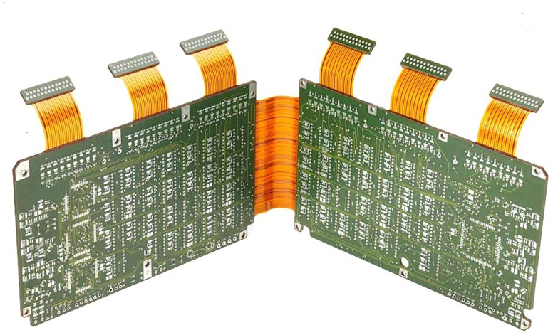
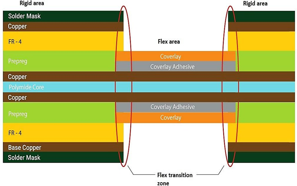
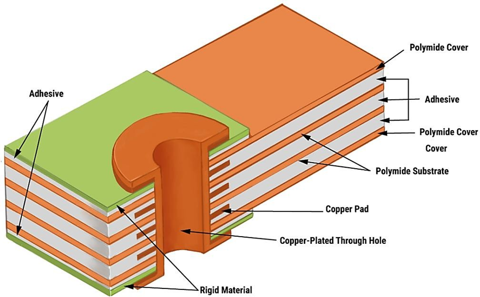
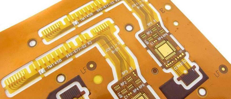
12. Flexible and Rigid-Flex
12.1. Flexible Circuit Fundamentals
Recommended Material:
- Polyimide base - Standard flexibility
- LCP (Liquid Crystal Polymer) - High-frequency applications
Thickness considerations:
LAYER COUNT |
THICKNESS |
BEND RADIUS |
|
1-LAYER |
0.05-0.1MM |
5× THICKNESS |
|
2-LAYER |
0.1-0.2MM |
10× THICKNESS |
|
4-LAYER |
0.2-0.4MM |
15× THICKNESS |
|
6+ LAYER |
0.4MM |
+20× THICKNESS |
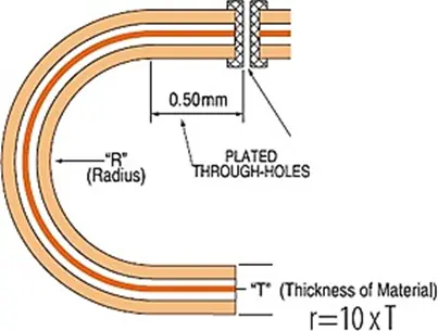
12.2. Bend Radius Calculation
Dynamic Flexing Requirements:
- Trace to trace - 0.1mm minimum
- Via to trace - 0.05mm minimum
- Pad to pad - 0.1mm minimum
- High voltage - Per safety standards
Static Bend Applications:
- § Board edge - 0.5mm keep-out zone
- § Mounting holes - 1.0mm clearance
- § Connectors - Mating clearance required
12.3. Rigid-Flex Transition Design
Stack-Up Considerations:
- Layer transitions in rigid sections only
- Via placement restrictions in flex zones
- Controlled impedance through transitions
Manufacturing Constraints:
- Minimum rigid section - 6mm width
- Flex section entry angle - <45°
- Stiffener overlap requirements - 1mm minimum
13. Component Guidelines
Different component types require specialized layout considerations.
13.1. BGA Escape Routing
VIA-in-PAD Technique:
- § Micro vias for high-density BGAs
- § Via filling requirements for assembly
- § Pad size reduction considerations
Escape Route Strategies:
BGA PITCH |
VIA SIZE |
ESCAPE |
REQ. LAYERS |
|
1.0MM |
0.1MM |
DIRECT ESCAPE |
2 LAYERS |
|
0.8MM |
0.1MM |
VIA-IN-PAD |
4 LAYERS |
|
0.5MM |
0.08MM |
MICRO VIA ONLY |
6+ LAYERS |
|
0.4MM |
0.08MM |
HDI TECHNOLOGY |
8+ LAYERS |
13.2 Crystal Oscillator Layout:
Critical Design Elements:
- Ground guard ring around crystal
- Minimum trace length to IC pins
- Load capacitor placement - <5mm from crystal
- Keep-out zones for switching signals
Frequency-Specific Considerations:
- Low frequency (<10MHz) - Standard layout rules
- Medium frequency (10-100MHz) - Guard rings essential
- High frequency (>100MHz) - Dedicated ground plane
13.3. Switch-Mode Power Supply Layout
Component Placement Priority:
- Input and output capacitors closest to switching IC
- Inductor placement for minimal loop area
- Feedback network routing away from switching nodes
- Thermal management for switching components
Critical Routing Guidelines:
- Minimize switching loop area
- Separate analog and power grounds
- Star ground connection point
- Input/output filtering isolation
Example Layout:
Buck converter requires <25mm² switching loop area for acceptable EMI performance at 1MHz switching frequency.
13.4 Connector Design Integration
High-Speed Connection Requirements:
- Stress relief design
- Board edge reinforcement
- Connector keep-out zones
- Assembly accessibility requirements
Power Connector Design:
- Stress relief design
- Board edge reinforcement
- Connector keep-out zones
- Assembly accessibility requirements
Mechanical Considerations:
- Stress relief design
- Board edge reinforcement
- Connector keep-out zones
- Assembly accessibility requirements
14. Design Verification
14.1. Design Verification Checklist
- DRC passes with zero violations
- Netlist verification against schematic
- Component placement review for assembly
- Thermal analysis for power dissipation
- Signal integrity simulation for critical nets
- Mechanical fit verification with enclosure
- Manufacturing file generation and review
14.2. Manufacturing Deliverables
- Gerber files
- Excellon drill files
- Pick and place files
- Bill of materials with manufacturer part numbers
- Assembly drawings with component orientations
- Fabrication notes with special requirements
14.3. Quality Metrics
- First-pass manufacturing yield >65%
- Assembly time optimization
- Test coverage maximization
- Field failure rate minimization
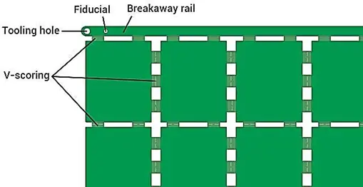
15. Penelization
Panelization combines multiple PCBs into a single manufacturing panel to optimize production efficiency, reduce costs, and improve handling during assembly processes.
15.1. Penelization Fundamentals
Definition and Purpose:
Panelization is the process of arranging multiple PCB copies on a single production panel for efficient manufacturing and assembly. This technique maximizes material utilization while maintaining manufacturability.
Primary Benefits:
- Cost reduction - Shared setup costs across multiple units
- Manufacturing efficiency - Batch processing advantages
- Handling improvement - larger panels easier to process
- Yield optimization - better material utilization ratios
Standard Panel Sizes:
PANEL SIZE |
DIMENSIONS |
TYPICAL APPLICATION |
|
SMALL |
50MM × 80MM |
PROTOTYPE RUNS |
|
MEDIUM |
100MM × 80MM |
PRODUCTION BATCHES |
|
STANDARD |
100MM × 160MM |
HIGH-VOLUME MANUFACTURING |
|
LARGE |
160MM × 100MM |
INDUSTRIAL APPLICATIONS |
15.2. Panel Layout Strategies
Array Configuration:
Strategic arrangement maximizes panel utilization:
Single Design Arrays:
- 1×2 arrangement - Simple doubling for small boards
- 2×2 configuration - Standard four-up panelization
- 3×3 layout - Nine-up for very small designs
- Custom arrays - Optimized for specific board dimensions
Mixed Design Pannels:
- Product family grouping - Related designs together
- Complementary sizing - Different boards filling panel space
- Test board inclusion - Quality control samples integrated
Spacing Requirements:
Critical clearances between boards:
- Minimum separation - 2.0mm between board edges
- Routing channels - 3.0mm for mechanical separation
- V-groove spacing - 0.5mm additional for scoring depth
- Tab connections - 1.5-3.0mm width depending on board thickness
15.3. Seperation Methods
V-Scoring (V-Grove):
Most cost-effective separation method:
Design Requirements:
- Straight line separation
- Optimal Board thickness - 0.8-3.2mm
- Minimum score depth - 1/3 of board thickness
- Edge distance - Minimum 0.5mm from components
Advantages and Limitations:
- Pros - Low cost, clean separation, high-speed process
- Cons - Straight lines only, board stress during separation
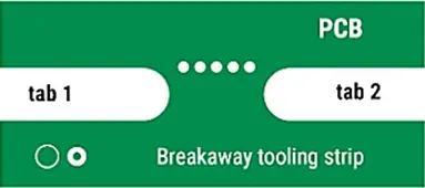
Tax Routing:
Flexible separation using small connecting tabs:
Tab Design Parameters:
- Tab width - 1.5-3.0mm typical
- Tab thickness - Full board thickness maintained
- Tab quantity - 3-6 tabs per board perimeter
- Tab placement - Avoid component areas and stress points
Tab Positioning Guidelines:
- Corner placement - Maximum structural support
- Edge centering - Balanced stress distribution
- Component avoidance - Minimum 2.0mm clearance
- Stress relief - Rounded tab connections preferred
House Bites (Perforated Tabs):
Alternative tab method using small drill holes:
- Hole diameter - 0.5mm typical
- Hole spacing - 0.5-1.0mm on centers
- Perforation length - 2-4mm typical
- Break strength - Easily separated by hand
15.4. Advanced Penalization Techniques:
Flex-Rigid Plane Design:
Special considerations for flexible circuits:
- Stiffener coordination - Support during assembly
- Bend relief integration - Stress management in panels
- Separation planning - Avoid damage to flex sections
- Handling fixtures - Custom tooling requirements
HDI Penelization:
High Density Interconnect considerations:
- Micro-via alignment - Registration across panel
- Sequential lamination - Process step coordination
- Yield optimization - Defect isolation strategies
- Test accessibility - Probing considerations for dense designs
Mixed Technology Panels:
Combining different board types:
- Thickness matching - Assembly line compatibility
- Material compatibility - Thermal expansion coordination
- Process optimization - Shared manufacturing steps
- Quality segregation - Different test requirements
16. Free Online Tools:
SATURN PCB TOOLKIT
https://saturnpcb.com/saturn-pcb-toolkit/
Comprehensive freeware resource for PCB-related calculations including current capacity of traces, via current, differential pairs and much more.
JLCPCB IMPEDANCE CALCULATOR
https://saturnpcb.com/saturn-pcb-toolkit/
Comprehensive freeware resource for PCB-related calculations including current capacity of traces, via current, differential pairs and much more.
PCBWAY IMPEDANCE CALCULATOR
https://saturnpcb.com/saturn-pcb-toolkit/
Comprehensive freeware resource for PCB-related calculations including current capacity of traces, via current, differential pairs and much more.
PCBWAY TRACE WIDTH CALCULATOR
https://saturnpcb.com/saturn-pcb-toolkit/
Comprehensive freeware resource for PCB-related calculations including current capacity of traces, via current, differential pairs and much more.
SIERRA CIRCUITS PCB TOOLS SUITE
https://www.protoexpress.com/tools/
Comprehensive suite including impedance calculator using 2D numerical solution of Maxwell's equations, via calculators, power distribution analyzers, and signal integrity tools.
ADVANCEDPCB TRACE WIDTH CALCULATOR.
https://www.advancedpcb.com/en-us/tools/trace-width-calculator/
Find the ideal trace width for PCB designs, ensuring optimal performance and reliability in circuit boards.
Summary
Professional PCB design integrates electrical engineering principles with manufacturing realities. Success requires systematic approach from schematic analysis through manufacturing handoff.
Key Success Factors
- Thorough preparation and component selection
- Strategic layer planning and routing
- Manufacturing constraint consideration
- Comprehensive design verification
- Clear documentation and communication
Continuous Improvement
- Design review feedback incorporation
- Manufacturing yield optimization
- Assembly process refinement
- Field performance monitoring
Next Steps
- Apply these techniques to actual projects
- Develop design rule libraries for common applications
- Build relationships with manufacturing partners
- Stay current with evolving technologies and standards
For further queries or internal training sessions, please reach out to the EIE Technical Support Team at info@eiengineerings.com
EIE Engineering Team
Innovating with Precision